If you’re evaluating a special PCB product for a high-complexity program, you’ve probably learned the hard way: not every “special PCB” supplier actually builds these boards in-house.
Below is a hands-on breakdown of three production-grade special PCB designs, evaluated from a hardware design and procurement perspective. We cover real-world use cases, core technical tradeoffs, and the specific verification checks you should run before sending an inquiry — no generic “high quality” claims, just the details that impact yield, reliability, and total program cost.
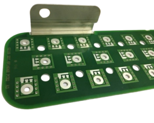
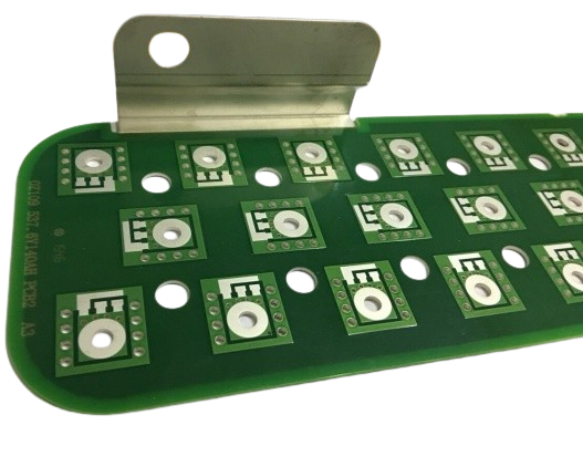
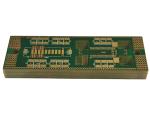
This board integrates precision-machined metal inserts laminated directly into the PCB stackup, rather than relying on surface-mounted terminals or separate bus bars. Each metal pad sits flush with the board surface, surrounded by standard FR4 dielectric and copper circuitry. An external metal mounting bracket extends from the board edge for structural attachment, combining electrical, thermal, and mechanical functions in a single assembly.
Typical end applications
Key technical characteristics
Procurement verification points: The biggest reliability risk with embedded metal PCBs is delamination at the metal-to-dielectric interface after thermal cycling. Before placing an order, confirm the supplier performs peel-strength testing on the metal-to-laminate bond, and can provide thermal cycling test data for the specific insert material and stackup. Also verify board flatness after lamination — mismatched CTE between metal and FR4 causes warpage that will break SMT yields if not controlled during pressing.
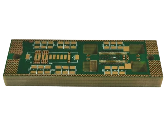
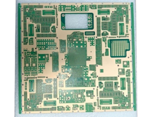
This ultra-thick, high-layer-count special PCB product is built for high-speed backplane and system interconnect applications. With dozens of signal, ground, and power layers stacked into a single rigid panel, it replaces multiple smaller boards and cable harnesses with one high-density interconnect structure. The dense via pattern and edge-plated contact arrays are typical of backplane designs used in network switches, server chassis, and semiconductor test systems.
Typical end applications
Key technical characteristics
Procurement verification points: High-layer-count boards live or die by lamination alignment and process control. Before selecting a supplier, confirm they run 100% AOI after every inner layer etch step — defects trapped between lamination cycles are invisible and irreparable. Also ask about warpage control methodology; thick multi-press boards have a strong tendency to bow and twist, which causes serious problems during connector press-fit and SMT assembly. For 40+ layer designs, you should also expect first-article cross-section analysis to verify plating uniformity and layer alignment.
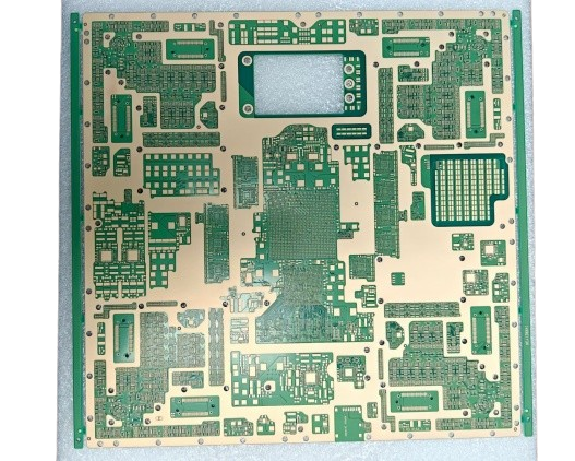
This 10-layer 2nd-order HDI PCB represents the most common high-density special PCB product used in modern industrial and embedded computing. Two sequential build-up layers on each side of an 8-layer core enable dense BGA fanout and high routing density without moving to a higher layer count through-hole board. Laser-drilled microvias, resin-filled via-in-pad structures, and fine trace geometries allow large pin-count ICs to be routed in a much smaller board area than standard through-hole technology can support.
Typical end applications
Key technical characteristics
Procurement verification points: The most common 2nd-order HDI failure modes are microvia cracking and resin voiding, neither of which is visible from the board surface. Confirm your supplier performs cross-section inspection on first articles to verify microvia plating integrity and resin fill quality. Also verify inner-layer registration accuracy; misaligned build-up layers create impedance deviations and signal integrity problems that are extremely difficult to diagnose after assembly.
| Product Type | Core Technology | Typical Layer Count | Primary Advantage | Typical Application | Relative Complexity |
| Embedded Metal PCB | Metal inlay/insert lamination | 2–8 layers | Ultra-low-resistance, high-current paths, integrated heat spreading | High-current power modules, BMS boards | High |
| Ultra-High Layer Count PCB | Multiple sequential lamination cycles | 20–50+ layers | Maximum signal/pin density in one board | Backplanes, test equipment, server infrastructure | Very High |
| 2nd-Order HDI PCB | Laser microvias + sequential build-up | 6–20 layers | Highest routing density per unit area | Embedded computing, high-density modules | High |
Special PCB technology is not a prestige upgrade. Every step up in complexity adds cost, lead time, and yield risk. You should only move to a more advanced special PCB type when a simpler technology genuinely cannot meet your requirements.
Cost-saving rule: Do not specify a higher complexity class than you need. A 12-layer standard through-hole board will almost always be cheaper, faster, and more reliable than a 10-layer 2nd-order HDI board — if the routing fits. Only step up in complexity when the simpler option is physically impossible.
A special PCB product is any printed circuit board built with materials, structures, or processes outside standard FR4 through-hole PCB capabilities. Common categories include HDI boards, heavy copper boards, metal core and embedded metal boards, high-layer-count backplanes, rigid-flex circuits, and high-frequency RF boards.
Embedded metal or metal-inlaid PCBs are used for very high current paths, localized heat spreading, and integrated mechanical mounting features. They eliminate the contact resistance of separate bus bars and improve thermal performance by moving heat directly into a solid metal conductor.
Standard production special PCBs commonly range from 2 layers up to 40–50+ layers for high-end backplane and test equipment designs. Higher layer counts require multiple lamination cycles and tighter process controls.
2nd-order HDI (high-density interconnect) means two sequential build-up layers are added to each side of a central core, enabling two levels of laser-drilled microvias. It supports finer pitch BGA fanout and higher routing density than 1st-order HDI, at a higher manufacturing cost.
Yes. We support prototyping through volume production for all major special PCB categories. Prototypes follow the same material and inspection standards as production builds to ensure valid performance validation.
If you have a high-complexity project and need to validate the right special PCB technology, send us your Gerber files, performance requirements, and target volume. Our engineering team will run a full DFM review, recommend the most cost-effective construction for your application, flag any manufacturability risks, and provide a transparent quotation with clear lead times.
We manufacture embedded metal, high-layer-count, HDI, heavy copper, and rigid-flex special PCB products for industrial, medical, automotive, and aerospace applications, with full compliance documentation for overseas markets. Contact us today to get started.
UpSmart PCBA brings nearly a decade of expertise to multilayer PCB manufacturing, serving industrial clients worldwide that demand tight tolerances, long-term durability, and batch-to-batch consistency.
We focus on custom PCB fabrication and full turnkey PCBA assembly. Your design files move straight through production into fully built, tested units ready for final installation — no fragmented handoffs between separate vendors. We scale seamlessly from small prototype runs to high-volume mass production, with end-to-end in-house capabilities spanning component sourcing, bare board manufacturing, in-process quality testing, and final packaging.
We build every order around three non-negotiables: quality, engineering rigor, and reliable turnaround. For our global industrial customers, this translates to simpler supply chains, fewer production disruptions, and electronic systems that deliver consistent performance over their full service life.
Email: sales@upsmartpcba.com
WhatsApp/Phone: +86 199 2656 6516