
If you design or source printed circuit boards, you know that trace geometry is far more than a cosmetic choice. Every bend, width transition, and spacing decision shapes signal integrity, EMI performance, and production yield. For teams working on modern high-speed designs, mastering high-speed PCB routing techniques means the difference between a board that works on the first spin and one that requires multiple costly revisions. Below is a breakdown of 8 widely used routing patterns, how they work, and the engineering trade-offs that define their use cases.
1. 45-Degree Mitered Routing (135° Included Angle)
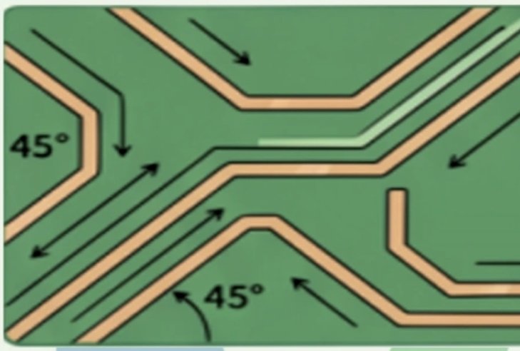
Shape
Trace corners are mitered at 45 degrees instead of sharp 90-degree right angles, creating a 135° internal turn. This is the default corner style in nearly all modern PCB design tools.
Why it is used
- Smoother impedance transition: Unlike 90° corners, which create an abrupt effective line-width increase and localized capacitance spike, 45° bends produce a gradual change that reduces signal reflection and overshoot.
- Lower EMI: Right-angle corners concentrate electric charge at the vertex, causing sharp radiated emissions. Angled corners spread charge more evenly and produce less radiated noise.
- Better etch fidelity: In conventional PCB etching processes, 45° corners etch more uniformly than sharp right angles, reducing side etching and burr formation.
- Cleaner layout: Neat, consistent angled routing makes design reviews faster and easier. As a baseline rule in PCB trace corner design best practices, 45° routing is the default for nearly all digital and mixed-signal designs.
2. Arc-Shaped / Curved Routing
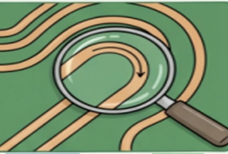
Shape
Corners use a smooth rounded arc, typically with a radius at least 3× the trace width. This is the standard corner style for very high-speed serial links and RF paths.
Why it is used
- Continuous impedance: A well-sized arc has effectively no width discontinuity, so characteristic impedance remains nearly constant through the bend. This makes curved routing ideal for serial links running at 10 Gbps and above, such as PCIe 5.0/6.0, USB4, and HDMI 2.1.
- Reduced harmonic radiation: The smooth profile produces lower high-frequency harmonic emissions than even 45° mitered bends.
- Lower mmWave loss: At millimeter-wave frequencies, arc bends minimize reflection and insertion loss compared to any angled corner.
3. 10° / 11° Skewed Routing
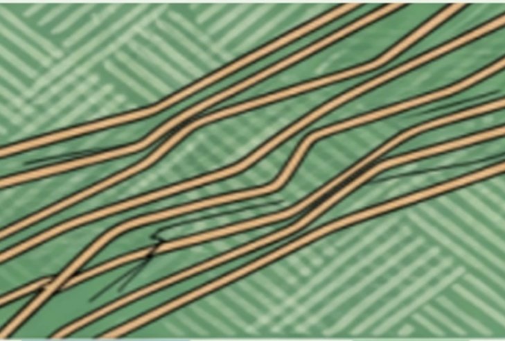
Shape
Traces are routed at a small fixed angle (typically 10° or 11°) relative to the board edge and the underlying fiberglass weave, rather than orthogonal 0°/90° alignment.
Why it is used
- Mitigates glass weave effect: Standard FR-4 laminates have an uneven woven fiberglass structure that causes localized dielectric constant variation, leading to differential skew and impedance fluctuation. Diagonal routing averages the dielectric seen by the trace across multiple weave positions, reducing mode conversion.
- Improved common-mode rejection: The effect is especially valuable for differential pairs operating above 10 Gbps, such as USB 3.2/4 and SFP+ interfaces.
- Tool-enabled implementation: Modern PCB design tools support arbitrary-angle routing, but skewed layouts must be paired with precise impedance control to deliver the full benefit.
4. Gradient / Tapered Traces
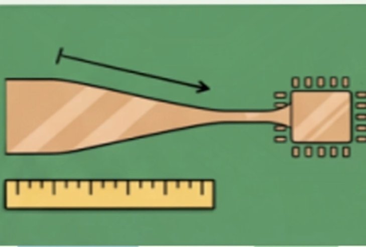
Shape
Trace width transitions gradually from wide to narrow (or vice versa) instead of stepping abruptly.
Why it is used
- Gradual impedance shift: When a signal path transitions from a wide structure (such as a power rail) to a narrow signal trace, a tapered section reduces the reflection coefficient compared to an instant width change.
- Smooth pad entry: Short tapered sections from fine traces to wider component pads reduce impedance jumps at device terminals.
- Improved mechanical reliability: Gradual width changes avoid stress concentrations that can cause copper delamination at sharp corners.
5. Teardrop Pad / Via Entries
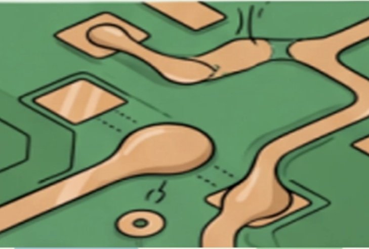
Shape
Teardrop-shaped copper fillets are added where traces connect to pads or vias, widening the connection point smoothly.
Why it is used
- Stress relief: Teardrops increase the copper connection area, reducing mechanical stress at the junction and preventing trace breakage from drill misalignment or thermal cycling.
- Better current distribution: The tapered shape evens out current density, avoiding hot spots at narrow neck-down points.
- Higher yield and reliability: Teardrops are a mandatory requirement for HDI boards, flexible circuits, and products deployed in high-vibration environments such as automotive and aerospace. In high-speed designs, teardrop size must be controlled to avoid adding excess capacitance that would degrade impedance. Proper PCB teardrop via design is one of the most impactful low-cost changes for improving long-term board reliability.
6. Serpentine / Zigzag Length Matching
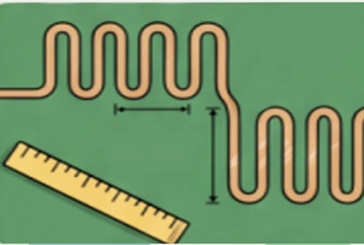
Shape
Traces are routed back and forth in a zigzag or U-shaped pattern to add controlled length.
Why it is used
- Length equalization: Parallel buses and multi-lane serial interfaces such as DDR memory and PCIe require matched flight times to preserve timing margin. Serpentine routing adds length to shorter paths so all signals arrive aligned.
- Differential pair skew correction: Small serpentine sections compensate for intra-pair length mismatch in differential routing.
- Key caveat: Serpentine sections must maintain a spacing of at least 4× the trace width to avoid introducing extra crosstalk, and the zigzag amplitude should be kept as small as practical. Accurate PCB serpentine length matching is essential for meeting setup/hold timing on high-speed parallel and serial buses.
7. Tightly Coupled Differential Pair Routing
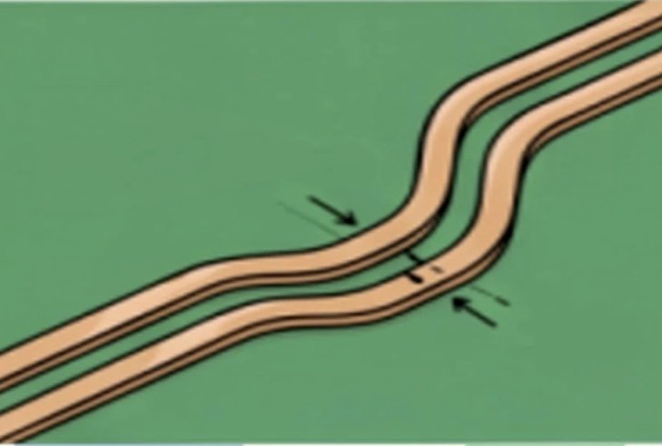
Shape
Two traces run parallel with matched length and constant spacing, with a gap typically ≤ 2× the trace width.
Why it is used
- Common-mode noise rejection: Tight coupling causes the electromagnetic fields of the two lines to cancel, reducing radiated emissions and improving immunity to external noise.
- Controlled differential impedance: Standard targets include 90 Ω for USB and 100 Ω for PCIe/Ethernet.
- Crosstalk caveat: Excessively tight spacing increases intra-pair crosstalk, so designs should follow the 3W rule for minimum separation to adjacent signals. Following established differential pair routing guidelines ensures consistent impedance and noise performance across production lots.
8. Guard Trace / Shielded Routing
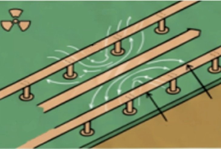
Shape
Ground traces are placed on both sides of sensitive signal paths, with ground vias stitched at regular ~10 mm intervals. Alternatively, a solid reference plane on an adjacent layer forms a Faraday shield.
Why it is used
- Dramatically reduced crosstalk: Guard traces confine fringing fields between the signal and ground paths, reducing crosstalk to neighboring nets by 10–20 dB.
- Lower radiated emissions: Shielded routing reduces outward radiation from high-speed or noisy signals.
- Typical applications: RF circuits, high-speed clock lines, and precision analog front ends such as ADC inputs all benefit from shielding. The tradeoff is increased routing area and higher via density.
Final Takeaway
No single routing pattern is universally best — each exists to solve a specific electrical, mechanical, or manufacturing challenge. For most designs, 45° routing is the reliable default, with curved bends, length matching, and differential coupling added selectively where signal speeds require them. Choosing the right pattern for each net is one of the core skills that separates good PCB layouts from great ones.
✅ Why Choose UpSmart PCBA?
UpSmart PCBA brings nearly a decade of expertise to multilayer PCB/PCBA manufacturing, serving industrial clients worldwide that demand tight tolerances, long-term durability, and batch-to-batch consistency.
We focus on custom PCB fabrication and full turnkey PCBA assembly. Your design files move straight through production into fully built, tested units ready for final installation — no fragmented handoffs between separate vendors. We scale seamlessly from small prototype runs to high-volume mass production, with end-to-end in-house capabilities spanning component sourcing, bare board manufacturing, in-process quality testing, and final packaging.
We build every order around three non-negotiables: quality, engineering rigor, and reliable turnaround. For our global industrial customers, this translates to simpler supply chains, fewer production disruptions, and electronic systems that deliver consistent performance over their full service life.
✅ Contact us
Email: sales@upsmartpcba.com
WhatsApp/Phone: +86 199 2656 6516