
If you work in PCB design, procurement, or fabrication, you’ve likely run into confusion about HDI order levels. What is the real difference between 1st-order, 2nd-order, and 3rd-order HDI PCBs? Does a higher total layer count always mean a higher HDI grade? How can you quickly tell the order from a stackup drawing or cross-section sample? This guide cuts through the jargon with clear, actionable definitions — no fluff, just rules you can apply on the job right away.
Core Rule (Most Important Point in This Guide)
The “order” of an HDI board is NOT the same as its total layer count. The only valid way to classify HDI level is by the number of sequential laser-drilled blind via build-up lamination cycles:
- ✅ 1st-order HDI = 1 build-up cycle with laser vias
- ✅ 2nd-order HDI = 2 build-up cycles with laser vias
- ✅ 3rd-order HDI = 3 build-up cycles with laser vias
Detailed Definitions & Stackup Structure by Order
Understanding the HDI PCB stackup structure guide is the foundation for correct ordering and costing. Each level adds one additional layer of laser-drilled interconnect capability.
1st-Order HDI (Entry Level)
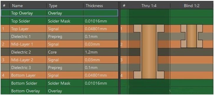
Standard stackup notation: 1+N+1. This is the most basic HDI configuration, with one build-up step and one laser drilling pass. Blind vias only connect the outer surface layer to the adjacent second layer. All through-holes are mechanically drilled, with no stacked via structure.
- Common stackup examples: 4-layer = 1+2+1; 6-layer = 1+4+1
- Key traits: simpler fabrication process, lower unit cost, higher production yield
- Typical applications: industrial control boards, general consumer electronics, products with BGA pitch ≥ 0.5mm
2nd-Order HDI (Mid-Tier Mainstream)
Standard stackup notation: 2+N+2. This grade uses two build-up steps and two laser drilling passes. Blind vias can reach down to the third layer from the surface and support both staggered and stacked via structures for much higher routing density.
- Common stackup examples: 6-layer = 2+2+2; 8-layer = 2+4+2
- Key traits: high wiring density, field-proven reliability; today’s dominant grade for premium consumer electronics
- Typical applications: flagship smartphones, tablets, thin laptops, boards with ~0.4 mm BGA pitch
3rd-Order HDI (High-End Advanced)
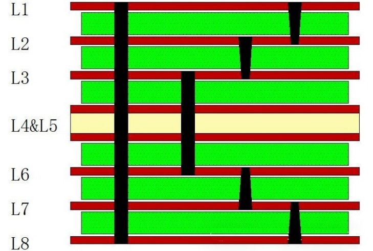
Standard stackup notation: 3+N+3. The highest standard HDI grade uses three build-up steps and three laser drilling passes. Blind vias can reach down to the fourth layer from the surface, support fully vertical stacked vias, and enable near-any-layer interconnect to push routing density to its practical limit.
- Common stackup examples: 8-layer = 3+2+3; 10-layer = 3+4+3
- Key traits: complex fabrication process, higher cost, extreme precision requirements
- Typical applications: 5G infrastructure, AI compute boards, high-end silicon packages with BGA pitch ≤ 0.3mm
3 Practical Ways to Identify HDI Order Level
If you’re wondering how to identify HDI order level from drawings or physical parts, these three methods cover nearly all on-the-job scenarios.
- Read the stackup drawing (fastest method)
- 1st-order: marked with 1+N+1 stack notation
- 2nd-order: marked with 2+N+2 stack notation
- 3rd-order: marked with 3+N+3 stack notation
- Inspect a cross-section sample (most accurate method)
- 1st-order: only L1-L2 blind vias on the outer layer; no via stacking
- 2nd-order: two tiers of blind vias (L1-L2 and L2-L3); may be staggered or partially stacked
- 3rd-order: three progressive via tiers (L1-L2-L3-L4); clear vertical stacked via structure
- Match to end application (quick estimate)
- General industrial / entry-level digital products → nearly always 1st-order
- Premium mobile / portable electronics → most often 2nd-order
- 5G, AI, ultra-fine-pitch silicon packages → 3rd-order high-density HDI
2 Common HDI Misconceptions to Avoid
❌ Myth 1: More total layers = higher HDI order
Fact: Total layer count and order level are completely independent. A 6-layer board can be either 1st-order (1+4+1) or 2nd-order (2+2+2). What defines the grade is the number of separate laser build-up cycles, not how many total layers the board has.
❌ Myth 2: More vias = higher HDI grade
Fact: Order level is defined by the number of independent laser build-up steps, not the total quantity of holes on the board. When blind via build-up layers are explained simply: each new order level adds one full lamination and drilling cycle, not just extra holes.
Quick Reference Cheat Sheet
Use this table for fast quoting, design review, and incoming inspection.
| HDI Order | Build-up / Laser Drilling Passes | Standard Stackup | Blind Via Reach | Typical Use Case |
| 1st-Order HDI | 1 | 1+N+1 | Outer layer ↔ Layer 2 | Industrial controls, general consumer electronics |
| 2nd-Order HDI | 2 | 2+N+2 | Outer layer ↔ Layers 2 & 3 | High-end phones, thin notebooks |
| 3rd-Order HDI | 3 | 3+N+3 | Outer layer ↔ Layers 2, 3 & 4 (stacked interconnect) | 5G hardware, AI compute, ultra-fine-pitch chip boards |
Final Takeaway
HDI order is defined by the number of laser blind via build-up lamination cycles — not the total number of board layers. 1st-order uses single-level blind vias, 2nd-order adds a second tier of vias, and 3rd-order enables deep stacked-via interconnect. Match the order to your BGA pitch and density requirements, and you’ll avoid over-specifying or under-specifying your next PCB program. For teams evaluating HDI PCB applications by density, choosing the minimum order that meets your routing needs is almost always the best balance of cost, lead time, and reliability.
✅ Why Choose UpSmart PCBA?
UpSmart PCBA brings nearly a decade of expertise to multilayer PCB/PCBA manufacturing, serving industrial clients worldwide that demand tight tolerances, long-term durability, and batch-to-batch consistency.
We focus on custom PCB fabrication and full turnkey PCBA assembly. Your design files move straight through production into fully built, tested units ready for final installation — no fragmented handoffs between separate vendors. We scale seamlessly from small prototype runs to high-volume mass production, with end-to-end in-house capabilities spanning component sourcing, bare board manufacturing, in-process quality testing, and final packaging.
We build every order around three non-negotiables: quality, engineering rigor, and reliable turnaround. For our global industrial customers, this translates to simpler supply chains, fewer production disruptions, and electronic systems that deliver consistent performance over their full service life.
✅ Contact us
Email: sales@upsmartpcba.com
WhatsApp/Phone: +86 199 2656 6516